CPU Design :
At the top level a computer consists of a CPU (central processing unit), memory, I/O components, with one or more modules of each type. These modules are interconnected in a specific manner to achieve the basic functionality of a computer i.e. executing programs. At the top level a computer system can be described as followes:
- describing the external behavior of each component i.e the data and the control signals that ir exchanges with other components
- describing the interconnection structure and the controls required
We are considering the Von Neumann architecture. Some of the basic features of this architecture are as follows:
- data and instructions are stored in a single read-write memory
- the contents of the memory are addressable by location
- execution occurs in a sequential manner (unless explicitly specified) from one instruction to the next
Top level components and interactions among them:
This experiment provides a single instruction CPU with built-in controller. A working memory has been provided to check the working principle of the CPU. The single instruction which this CPU supports is SBN (subtract and branch if negative). The format of this instruction is:
- SBN a,b,c Mem[a] = Mem[a] - Mem[b] if(Mem[a] < 0) goto c
- a, b, c are 4 bit addresses
- Mem[a] denotes the contents of memory address a
In this experiment, no I/O module has been included for the purpose of simplicity. The working memory should contain the programm and data in binary format. The CPU executes the programm. For halting, it uses self loop, no other halt instruction is provided.
CPU Design :
Basic stage
Multiple choice questions:
Subjective questions:
- What is a stored program computer?
- What general catagories of functions are specified by computer instructions?
- What are the possible states that define the instruction execution?
- What is wired AND operation?
Advanced stage
Multiple choice questions:
Subjective questions:
- What is the maximum memory address space that the processor can access directly if it is connected to a 16-bit memory address?
- What are the main components of any general purpose computer?
- What is the advantage of multiple-bus architecture rather than using single-bus architecture?
CPU Design:
Procedure to perform the experiment:CPU Design
- Start the simulator as directed.This simulator supports 5-valued logic.
- To perform the experiment on the given modules, we need the CPU, the working memory with a program and data loaded, a clock input, Bit switch(to give input,which will toggle its value with a double click), Bit displays(for seeing output), wires.
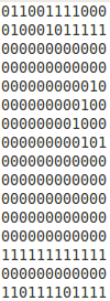
- Load memory: click on the load memory button in the left pane. you can either load the memory by filling the form or you can directly load the program form a text file. The memory provides 4-bit address space and 12 bit data word, thus providing 16 memory address starting from 0000 to 1111. For loading from file, the file should contain only binary values, it must contain 16 lines, each line containing the content to be stored in the corresponding memory address. For example, content of first line will be loaded to the 0000 address of the memory, similarly, the second line will correspond to the 0001 address and so on, finally the content of last line will be fed to the 1111 address. The progrm should use self loop for halting, for example, the instruction stored at address 1010 will cause self loop execution, if it content of a has -1 in binary format (in 2's complement), the content of b has 0 and c is 1010, then once the execution reaches to this 1010 address, it will finally point to itself.
- Instantiating the memory: after loading the memory, click on the memory component from the computer design drawer in the palette of the simulator then click on the position of the design editor where you want to put the component(no drag and drop, simple click will serve the purpose).
- The pin configuration of the component is shown whenever the mouse is hovered on any canned component of the palette or pressing the show pin configuration button on the toolbar will show it constantly in the left pane. Pin numbering starts from 1 and from the bottom left corner(indicating with the circle) and increases anticlockwise.
- Pin configuration of the memory module:
- Input pins (upper terminals): memory enable : 30, R/W' : 29, address : 25-28, data : 13-24 (13 is LSB)
- Output pins(lower terminals): data output : 1-12 (1 is MSB)
- Instantiate the CPU from the computer design drawer in the palette of the simulator then click on the position of the design editor where you want to put the component.
- Pin configuration of the CPU:
- Input pins (upper terminals): data input : 20-31 (20 is MSB) ,clock input : 19
- Output pins(lower terminals): memory enable : 1, R/W' : 2, address : 3-6( 3 is MSB), data output : 7-18 (7 is MSB)
- To connect any two components select the Connection menu of Palette, and then click on the Source terminal and click on the target terminal. According to the following diagram connect all the components. Connect the memory outputs to the input terminals of the CPU, specified datapath outputs to the inputs of the controller, the clock input, Bit switches with the inputs and Bit displays component with the outputs (from Display and Input drawer of the pallet,if it is not seen scroll down in the drawer). After the connection is over click the selection tool in the pallete.
- Start clock and observe the behavior of the CPU.See the content of memory by clicking show memory button in the left pane. Observe how the program is executing sequentially and modify the data content as per the program.
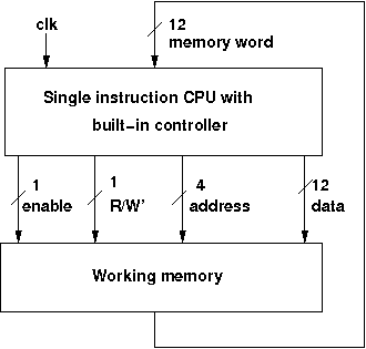
Objective of CPU design:Our main objective for this experiment is to show the basic top level functionality, organization and architecture of a computer.This top level structure and function of a basic computer is important because of its explanatory power in understanding the nature of a computer. A grasp on these basic structure and functionality will provide insight into system bottolnecks, alternative pathways. Because in many cases, requirement of greater system power and fail-safe capabilities are achieved by changing the system design rather than changing the speed and reliability of individual components. So we have designed a single instruction CPU which contains a controller. A working memory has been given to examine the behavior of the CPU. The memory will contain the program in binary format which will be executed by the CPU. Through this, students can observe the behavior of a basic CPU and as well as a computer. The I/O modules have not been included in the system for the purpose of symplicity.
Recommended learning activities for the experiment: Leaning activities are designed in two stages, a basic stage and an advanced stage. Accomplishment of each stage can be self-evaluated through the given set of quiz questions consisting of multiple type and subjective type questions. In the basic stage, it is recommended to perform the experiment firstly, on the given encapsulated working module, secondly, on the module designed by the student, having gone through the theory, objective and procuder.
By performing the experiment on the working module, students can only observe the input-output behavior.
Where as, performing experiments on the designed module, students can do circuit analysis, error analysis in addition with the input-output behavior.
It is recommended to perform the experiments following the given guideline to check behavior and test plans along with their own circuit analysis. Then students are recommended to move on to the advanced stage. The advanced stage includes the accomplishment of the given assignments which will provide deeper understanding of the topic with innovative circuit design experience. At any time, students can mature their knowledge base by further reading the references provided for the experiment.
color configuration of wire for 5 valued logic supported by the simulator:
- if value is UNKNOWN, wire color= maroon
- if value is TRUE, wire color= blue
- if value is FALSE, wire color= black
- if value is HI IMPEDENCE, wire color= green
- if value is INVALID, wire color= orange
Test plan :
Load the memory according to the following figure, then start clock and observe the behavior of the CPU. See the content of memory by clicking show memory button in the left pane. Observe how the program is executing sequentially and modify the data content as per the program.
Assignment Statements :
- Design a single instruction CPU
- Design a CPU with more instructions
CPU Design::
General guideline to use the simulator for performing the experiment:
- Start the simulator as directed. For more detail please refer to the manual for using the simulator
- To add the logic components to the editor or canvas (where you build the circuit) select any component and click on the position of the canvas where you want to add the component
- The pin configuration is shown when you select the component and press the 'show pinconfig' button in the left toolbar or whenever the mouse is hovered on any canned component of palette
- To connect any two components select the connection tool of palette, and then click on the source terminal and then click on the the target terminal
- To move any component select the component using the selection tool and drag the component to the desired position
- To give a toggle input to the circuit, use 'Bit Switch' which will toggle its value with a double click
- Use 'Bit Display' component to see any single bit value. 'Digital Display' will show the output in digital format
- undo/redo, delete, zoom in/zoom out, and other functionalities have been given in the top toolbar for ease of circuit building
- Use start/stop clock pulse to start or stop the clock input of the circuit. Clock period can be set from the given 'set clock' button in the left toolbar
- Use 'plot graph' button to see input-output wave forms
- Users can save their circuits with .logic extension and reuse them
- After building the circuit press the simulate button in the top toolbar to get the output
- If the circuit contains a clock pulse input, then the 'start clock' button will start the simulation of the whole circuit. Then there is no need to again press the 'simulate' button
- If you are using linux platform then click on 'Linux(32 bit)' or if you are using then click on 'Windows(32 bit)'
If you are using linux platform then click on 'Linux(32 bit)' or if you are using then click on 'Windows(32 bit)'
Linux(32 bit)
Windows(32 bit)
A basic computer:
Back
A basic computer:
Back
Click here to download the older version of simulator
Click here to download the new version of simulator
OR
Launch the older version of Simulator
Launch the new version of Simulator
Once the simulator is downloaded, open the command prompt, then go to the directory where you have saved it using cd command and then give the following command to run the simulator:
java -jar coaSimulator.jar
Click here to download the older version of simulator
Click here to download the new version of simulator
OR
Launch the older version of Simulator
Launch the new version of Simulator
Once the simulator is downloaded, open the command prompt, then go to the directory where you have saved it using cd command and then give the following command to run the simulator:
java -jar Simulator.jar
CPU Design :
References :
Books:
- Computer Organization and Architecture - William Stallings
- Computer System Architecture - M. Morris Mano
- Computer Architecture and Organization - John P. Hayes
- Digital Logic and Computer Design - M. Morris Mano. Pearson Education - Prentice Hall.
- Digital Principles Foundation of Circuit Design and Application - Arun Kumar Singh. New Age Publishers.
- The Art of Electronics - Paul Horowitz and Winfield Hill (1989). Cambridge University Press
- Modern Dictionary of Electronics - Rudolf F. Graf (1999). Newnes
Web Sites:
Virtual Lab is an initiative of Ministry of Human Resource and Development(MHRD) under
National Mission of Education through ICT to provide an interactive environment over the internet for creating and conducting different laboratory experiments by sharing the costly
equipments and the resources.
For more information about the Virtual Lab,please visit http://www.vlab.co.in/
Developers of Logic Design and Computer Organization Virtual
Lab
- Dr. Chittaranjan Mandal
Professor, Computer Science & Engineering
Professor, Information Technology
IIT Kharagpur
- Gargi Roy
Senior Project Assistant
- Devleena Ghosh
Target Audience:
Under graduate students.
Courses Aligned With:
Computer organization and artitecture.
Pre-requisite Softwares:
- 32 bit java runtime environment and java 1.6 or above
- Recommended browser: mozilla firefox, google chrome
Objectives:
The Objective is to Expose the students to the various key aspects of Logic Design and Computer Organisation by enabling them to perform FPGA based prototyping of experiments with support of a virtual environment. The primary need
for virtualisation here is multifold.
- Digital Logic and Computer Organisation happens to be a Core Course in most of the Undergraduate Curricula of the entire Electrical Sciences Discipline(Computer Science / Engg., Electronics, Electrical) etc.
- Many colleges/institutes cannot procure sufficient number of FPGA boards for their students.
- Even when such FPGA boards are available, making them available round the clock is difficult.
- Expert help is required to effectively use these FPGA boards and such help can be easily channeled through a virtual environment.
- Helps to standardize the set of Experiments to a large extent.
Feedback:
To give your feedback please visit the following link-
Sponsered by MHRD
(NME-ICT) .
Contact Information:
Mailing Address and Contact Information:
Department of Computer Science & Engineering, IIT Kharagpur
Office : +91-3222-2882255
Postal Address:
Indian Institute of Technology Kharagpur, Kharagpur - 721302, INDIA
Telephone Number +91-3222-255221 | FAX : +91-3222-255303
Tutorial on UI for lab:
Introduction:
- The simulator contains a pallete on the right hand side. This pallete contains all the components and tools . Tools are used to act up on the components. Different tools:
- Selection tool- used for selecting components
- Marquee tool- used for selecting many components at a time by draggiung the mouse in the design area(editor).
- Connection tool- used for connecting components
- Components have been catagorized according to their functionality and put into different drawers in the pallete. The area under every drawer is scrallable, if you are unable to see all the components in a particular drawer just click on the area and scroll. Different drawers:
- Circuits- contains 8 and 16 terminal circuits and flow container which can hold other circuit components.
- Logic gates- contains all kinds of basic logic gates.
- Display and inputs- contains all kinds of component needed to give input to the circuit and displaying outputs of the circuit.
- Adders- contains different types of adder circuits.
- Sequential ckt- contains basic flipflops for designing sequential circuits.
- Other Components- contains different kinds of components like decoders, multiplexers, arithmetic logic units(ALU), memory elements(RAM cell) required to design combinational circuits.
- To add the components to the editor select any component(first click on the selection tool then click on the desired compoent) then finally click on the position of the editor window where you want to add the component.
- The pin configuration of a component is shown whenever the mouse is hovered on any canned component of the palette. Pin numbering starts from 1 and from the bottom left corner(indicating with the circle) and increases anticlockwise.
- To connect any two components select the Connection tool in the palette, and then click on the Source terminal and click on the target terminal(no drag and drop, simple click will serve the purpose). After the connection is over click the selection tool in the pallete.
- To move any components select the Selection Mode and drag the component after selecting it.
- If needed select any component in the editor while designing your circuit and use Undo, Redo, Delete,Zoom in, Zoom out buttons to get corresponding functionalities. Open and Save options are under development.
- As the automated clock is under development and the simulator is under modification for sequencial circuits, for the time being please use individual clock(Bit switch which toggle its value with a double click) for each flipflop.
- The simulator is currently under modification for sequential circuits, now it is working properly for combinational circuits but may not give proper output for sequential circuits.
Description of Components:
General components:
- Digital display: it can be used to give input and as well as to see the output in the decimal format, its right most terminal is the LSB(least significant bit) and the left most terminal is the MSB(most significant bit), in the editor after selecting a particular digital display you can use 'Increment LED' and 'Decrement LED' buttons in the top left corner of the simulator to increment and decrement its value respectively.
- Bit display: it displays a single bit value.
- V+: it gives 1 as input.
- Ground: it gives 0 as input.
- Bit switch: it gives 1/0 input, it toggels its value with a double click.
Specific components:
Specific components:
Pin numbering starts from 1 and from the bottom left corner(indicating with the circle) and increases anticlockwise. Pin configurations of all the components-
Adder drawer:
- Half adder: i/p: 5,8 o/p: sum=4, carry=1
- Full adder: i/p: 5,6,8 o/p: sum=4, carry=1
- RCA 4 bit: (4 bit ripple carry adder) i/p: A0=13,A1=14,A2=15,A3=16; B0=17,B1=18,B2=19,B3=20; C0=21 o/p: S0=12,S1=11,S2=10,S3=9,Cout=8
- Wallace tree adder: (adds 3 4-bit numbers) i/p: A0=13,A1=14,A2=15,A3=16; B0=17,B1=18,B2=19,B3=20; C0=21,C1=22,C2=23,C3=24 o/p: S0=12,S1=11,S2=10,S3=9,Cout=8
Sequencial ckt drawer:
- RS flipflop: i/p: R=5, S=8, Clk=7 o/p: Q=4, Q'=1
- D flipflop: i/p: D=5, Clk=8 o/p: Q=4, Q'=1
- T flipflop: i/p: T=8, Clk=7 o/p: Q=4, Q'=1
- JK flipflop: i/p: J=5, K=8, Clk=7 o/p: Q=4, Q'=1
Other components drawer:
- 2:4 Decoder: i/p: A0=5,A1=7 o/p: D0=4,D1=3,D2=2,d3=1
- 2:4 Decoder with enable: i/p: A=6,B=5, Enable=8 o/p: D0=4,D1=3,D2=2,d3=1
- 4:1 Mux: i/p: I0=9,I1=10,I2=11,I3=12,S0=13,S1=14 o/p: F=8
- Combinational Multiplier: i/p: multiplicand: A0=13,A1=14,A2=15,A3=16 Multiplier: B0=9,B1=10,B2=11,B3=12 o/p: S0=8,S1=7,S2=6,S3=5,S4=4,S5=3,S6=2,S7=1
- ALU 1 bit: i/p: A0=9, B0=10, C0=21 S0=12,S1=13 o/p: F=8, Cout=7
- 4 bit ALU: i/p: A0=13,A1=14,A2=15,A3=16; B0=17,B1=18,B2=19,B3=20; C0=21;S0=22,S1=23 o/p: F0=12,F1=11,F2=10,F3=9,Cout=8
- 16 bit ALU: i/p: A1=13,A2=15; B1=14,B2=16; Cin=9,S0=12,S1=11,S2=10 o/p: Cout=6,F2=7,F1=8
- RAM Cell: i/p=5, select=8, R/W'=6, o/p=4, R/W'=1 for read operation, R/W'=0 for write operation
- IC Memory: R/W'=16 Memory Enable=15, Address i/p=14,13 Data i/p=12,11,10 Data o/p=6,7,8 R/W'=1 for read operation, R/W'=0 for write operation
- Direct Mapped Cache:
- pin-32= S(selects whether user wants to perform cache write or cache mapping)
- pin-31= R/W'A(selects whether user wants to input the address or cache mapping)
- pin-30=A3, pin-29=A2, pin-28=A1, pin-27=A0 (thise 4 pins are used to give address input). A3 is the most significant bit and A0 is the least significant bit. A3 and A2 will be compared with the tag. A1 and A0 will select the corrsponding set.
- pin-26= R/W'D(selects whether user wants to input in the set of cache or cache mapping)
- pin-25= M1, pin-24=M0 (M1 is the most significant bit and M0 is the least significant bit). thiese two bits are used for cache writhe purpose, it selects the particular set of which user wants to give inputs to the valid bit, tag bits and data bits.
- pin-23= Den(this is an enable input which has to set for any write purpose in the cache).
- pin-21= valid bit
- pin-20= T1, pin-19=T0 (T1 is the most significant bit and T0 is the least significant bit). These are tag bits.
- pin-18= D1, pin-17=D0 (D1 is the most significant bit and D0 is the least significant bit). These are data bits.
- pin-14= Hit/Miss bit(if it gives 1 then hit otherwise miss)
- pin-15= F1, pin-16=F0 (F1 is the most significant bit and F0 is the least significant bit). These are output data bits and will be given only when there is a hit.
- Essential pin configurations for writing in cache: S=1, R/W'A=0, R/W'D=0, Den= 1
- Essential pin configurations for cache mapping: S=0, R/W'A=1, R/W'D=1, Den= 0
Hide specific components
Testing process:
- To test your circuit give some input(through Digital display or Bit switch or V+ or Ground), if you use the Digital display or Bit switch you can then give different input to you circuit through incrementing/decrementing the Digital display or double clicking the Bit switch, the other two gives constant inputs.
- to see the output, connect Digital display or Bit display to the output terminals of your circuit.
Go to the Top
Frequently Asked Questions:
What is virtual lab?
The Virtual Laboratory is an interactive environment for creating and conducting simulated experiments: a playground for experimentation. It consists of domain dependent simulation programs, experimental units called objects that encompass data files, tools that operate on these objects.
What are the advantages of virtual lab?
Virtual Logic Design and Computer Organisation lab enables students to perform FPGA based prototyping of experiments with support of a virtual environment. The primary need
for virtualisation here is multifold.
- Digital Logic and Computer Organisation happens to be a Core Course in most of the Undergraduate Curricula of the entire Electrical Sciences Discipline ( Computer Science / Engg., Electronics, Electrical ] etc.
- Many colleges/institutes cannot procure sufficient number of FPGA boards for their students.
- Even when such FPGA boards are available, making them available round the clock is difficult.
- Expert help is required to effectively use these FPGA boards and such help can be easily channeled through a virtual environment.
- Helps to standardize the set of Experiments to a large extent.
What is eclipse platform?
Eclipse is a Java-based, extensible open source development platform. By itself, it is simply a framework and a set of services for building a
development environment from plug-in components. Eclipse comes with a standard set of plug-ins, including the Java Development Tools (JDT).
Which framework is used to develop the application?
We have used the eclipse gef framework. The Graphical Editing Framework (GEF) allows developers to take an existing application model and quickly create a rich graphical editor.
What is platform independent application?
Applications that run under particular operating systems and/or particular hardwares are called platform dependent application whereas platform independent applications can run in any operating environment.
What are the experiments which can be performed by the Virtual Logic Design and Computer Organization lab?
The experiments that will be supported by this lab are given below:
- Design of a ripple carry adder
- Design of a carry-look-ahead adder
- Design of registers and counters
- Design of a wallace tree adder
- Design of combinational multipliers
- Design of a Booth’s multiplier
- Design of an ALU
- Design of memory units
- Design of direct mapped cache
- Design of associative cache
- Design of combinational dividers
- CPU design