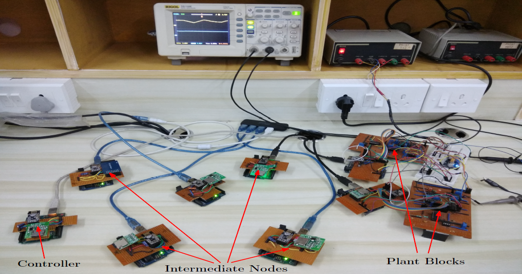
Wireless CPS Testbed
A networked CPS consists of multiple nodes with different roles (e.g., plant, controller, intermediate node, router, etc.), which all require their customly developed firmware. Moreover, these nodes have to be interconnected through a wireless network, which requires further design effort.
Our CPS hardware testbed can be developed with minimalistic development effort and is highly scalable. Extra hardware can be added or existing devices can be upgraded easily, without requiring a time-consuming software redesign. For example, a small network can be easily transformed into a larger network by adding additional nodes. The only required step is the GUI-driven configuration, specification and automated regeneration of the software. Furthermore, different network topologies, e.g., single- and multi-hop, can be generated easily.
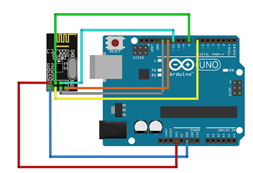
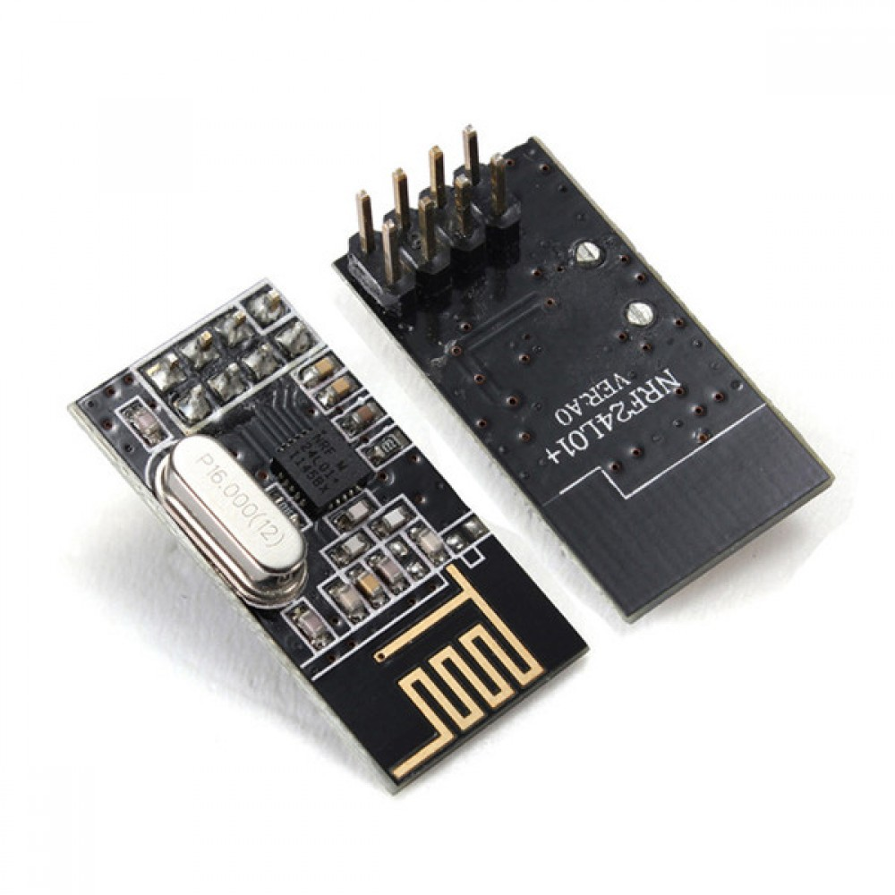
Each node in the network is formed by a widely-used Arduino UNO microcontroller, which is equipped with a nRF24L01+ RF module. Some of these nodes take over the role of a controller, whereas others are equipped with some physical setup to be controlled (the physical plant), or act as intermediate nodes that relay information. The firmware images are deployed over-the-air, which reduces the effort of testbed deployment.
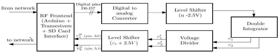
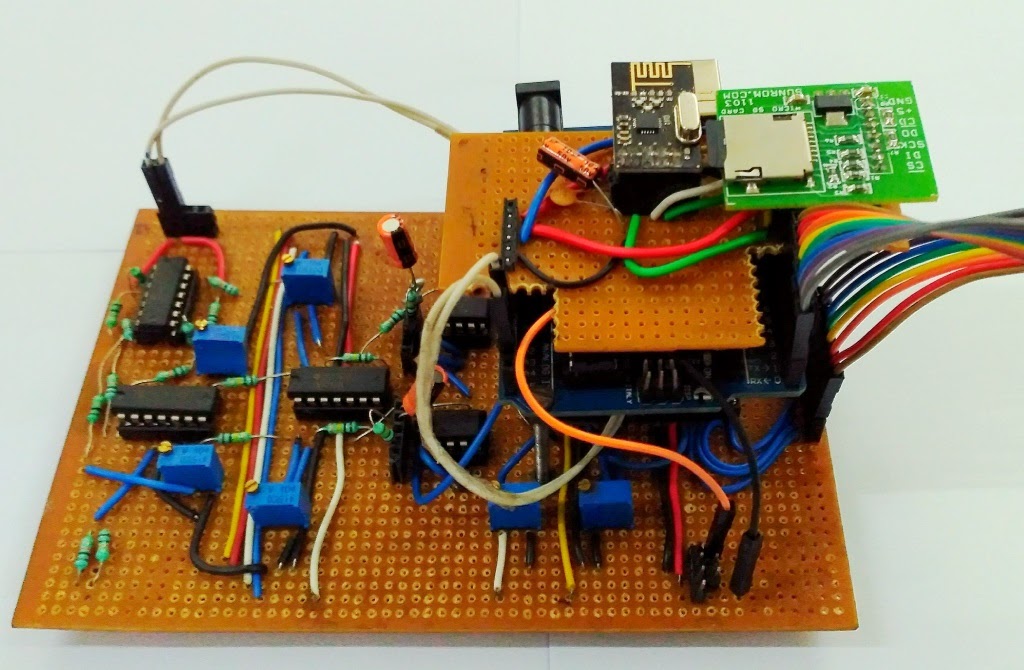
We consider a Double Integrator Circuits (DIC) as the first physical plant supported by our testbed. It consists of two operational amplifiers (UA741) connected in series, thereby computing the integral over the integral of the input signal of the first amplifier. A complete plant block developed in our testbed, is shown in the given figures. It consists of a DIC, two level shifters, one voltage divider and a radio-frequency (RF) front-end.
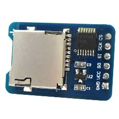
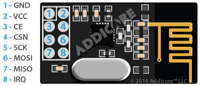
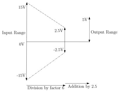
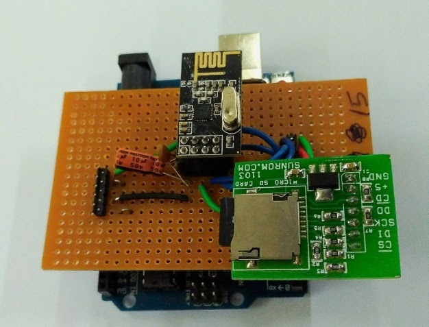
The DIC model is realized with the UA741 as the Op-amps which produce a voltage range from +15V to -15V in output of DIC. Since the analog input pins on the microcontroller of the plant block can tolerate incident voltage in the range 0 - 5V, we need to scale the entire output range of DIC. The voltage divider divides the DIC's output voltage by factor of six to achieve the voltage range of [-2.5V,2.5V]. Next in lower level shifter they are added by 2.5V to make the incident voltage in the range 0 - 5V. To provide both positive and negative actuation values in the control input u, the range of 0-5V of control signal values received by plant Arduino and sampled at output pins D0-D7 are converted into the range [-2.5V,2.5V] in upper level shifter. The RF interface we choose for our testbed is the Nordic Semiconductors NRF24L01+ transceivers operating at the 2.4GHz ISM band. The SD interface used in the testbed is the generic SPI (Serial peripheral Interface) based SD module. The purpose of it is to provide persistent storage for various data. Both the RF transceiver and SD Interface communicate with microcontroller over SPI bus.
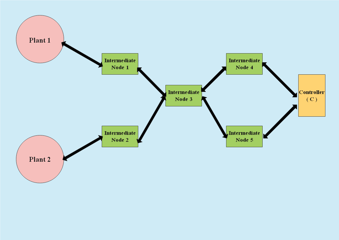
The underlying hardware design for the controller as well as all intermediate nodes include a microcontroller, RF interface and SD module. The functionality of RF interface, and SD module is same as described for plant block. In intermediate nodes, the microcontroller is configured by the software tool to implement the buffers for storing and forwarding the plant output and control input between plants and controllers in their designated time slots as defined in the network schedules. The microcontroller in control node is programmed to receive respective plant outputs from the network, compute the control input using the associated control law and transmit it back over the network. The node implements a cyclo-static schedule executing controllers for different plants in a specific sequence.
The clock node consists of the same hardware and provides a clock signal to which all nodes are synchronized. With a period equivalent to the slot length, a clock signal is broadcasted to all nodes. In addition, the clock node is also responsible for orchestrating the collection of experimental data over the network.

Given the GUI-based CPS specification, firmware for each node is generated and deployed by the software tool. This firmware is also responsible for controlling the connectivity. The wireless communication is built on top of the Enhanced ShockBurst protocol, which operates in the ISM band (2.400 - 2.4835 GHz). We use an over-the-air data rate of 250 Kbit/s. As a congestion control mechanism, the NRF24L01P RF module implements up to 6 logical addresses (called pipes) for listening in parallel. A module can only transmit to one pipe at a time. In our setup, three pipes are maintained by each RF module for handling the global clock, plant/control and log data. Channel arbitration is done based on time-multiplexed media access. Time is subdivided into 10ms-slots and the clock node transmits a synchronization pulse to all nodes every 10ms. Upon receiving the clock pulse, each node first checks if there is any data to be processed. A node may initiate a transmission, whenever the current slot is assigned to this node for transmission. Similarly, a node will listen for incoming transmissions from other nodes during the appropriate slots. The clock node can also initiate data logging on a node, or request the transmission of the previously logged data.