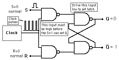
Set-reset (SR) latch
SR latch using NAND gates

SR latch using NOR gates

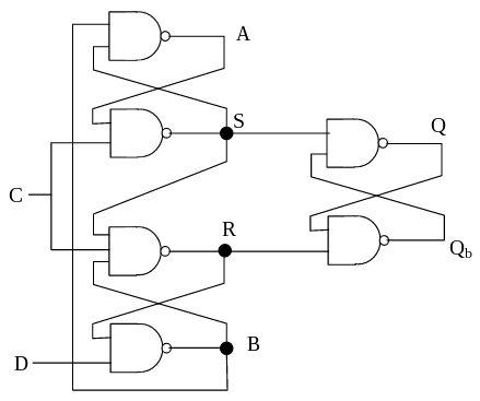
Clocked SR latch (using NAND gates)
 |
| Truth table
| | Clk | S | R | Q
| | 1 | 0 | 0 | No change
| | 0 | 1 | 0
| | 1 | 0 | 1
| | 1 | 1 | Invalid
| | 0 | No change
| |
Chatterless switch

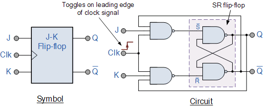
JK flip flop
Basic JK FF
 |
| Truth table
| | Clk | J | K | Q | Q New
| | 1 | 0 | 0 | — | No change
| | 0 | 1 | 0 | 0 (NC)
| | 0 | 1 | 1 | 0 (Q'→1)
| | 1 | 0 | 0 | 1 (Q→1)
| | 1 | 0 | 1 | 1 (NC)
| | 1 | 1 | 1 | 0 (Q'→1)
| | 1 | 1 | 0 | 1 (Q→1)
| | 0 | No change
|
|
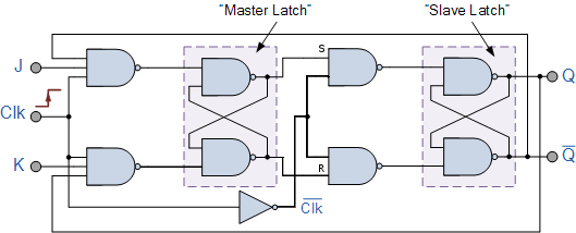
Master-slave JK FF
 |
| Truth table
| | Clk | J | K | Q | Q New
| | 0 | Master: NC; MLat → SLat
| | 1 | Slave: NC
| | 1 → 0 | 0 | 0 | — | MLat → SLat
| | 0 | 1 | — | 0 (S=0, R=1)
| | 1 | 0 | — | 1 (S=1, R=0)
| | 1 | 1 | 1 | 0 (S=0, R=1)
| | 1 | 1 | 0 | 1 (S=1, R=0)
| |
| Active clock edge: 1 → 0 (falling) |
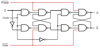
D FF with asynchronous preset and clear
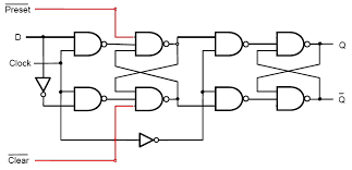
D FF with synchronous preset and clear
Residual problem with above DFF
- Let the gate delay be Δ
- Let D=0, Clk=1
- Let D=1 and just before Δ time, Clk=0
- Master latch has the invalid input combination of 00
- Before valid inputs could appear at the steering gates of the master latch, Clk=0
- Now, invalid input combination of 11 is presented to the slave steering gates,
with Clock'=1
- Slave latch has the invalid input combination of 00
- Output of DFF is indeterminate
Problem may be avoided if D remains steady when Clk=1, allowed to change
only when Clk=0
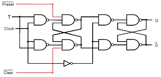
T FF with preset and clear
Similar to DFF, but J and K terminals tied (J=K=1)
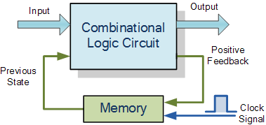
Huffman model
Schematic diagram
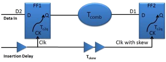
Setup and hold times
-
Setup time
-
It is defined as the minimum amount of time before the active clock edge by which
the data must be stable for it to be latched correctly;
any violation in this required time causes incorrect data to be captured and is known as a setup violation
-
Time available for data at D2 to reach D1 after active clock edge
-
Tclk + Tskew - Tsetup
-
Time needed for date to reach D1 from D2 after active clock edge
-
Tc2q + Tcomb
-
Resulting constraint
-
Tc2q + Tcomb ≤
Tclk + Tskew - Tsetup
Tc2q + Tcomb + Tsetup ≤
Tclk + Tskew
-
Hold time
-
It is defined as the minimum amount of time after the active clock edge by which
the data must be stable for it to be latched correctly;
any violation in this required time causes incorrect data to be captured and is known as a hold violation
-
Minimum time for data at D2 to reach D1 after active clock edge
-
Tc2q + Tcomb
-
Time for data to remain steady at D1 after active clock edge
-
Tskeq + Thold
-
Resulting constraint
-
Tc2q + Tcomb ≥
Tskeq + Thold
Example for setup and hold times
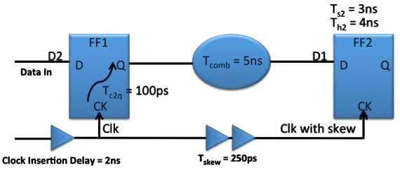
- What is the minimum clock frequency?
- Tclk + Tskew ≥ Tc2q + Tcomb + Ts2
- Tclk + 0.25ns ≥ 0.1ns + 5ns + 3ns
- Tclk ≥ 7.85ns
Positive clock edge triggered DFF
|
| Transition table
| | C | D | R | S
| RΔ | SΔ | QΔ
| | 0 | — | — | — | 1 | 1 | Q
| | 1 | 0 | 1 | 1 | 0 | 1 | 0
| | 1 | 1 | 1 | 1 | 0 | 1
| | — | 0 | 1 | 0 | 1 | 0
| | — | 1 | 0 | 1 | 0 | 1
| | — | 0 | 0 | 1 | 0 | 1
|
|
-
SΔ = (C · A)' = C'+ A'=
C' + B · S =
C' + (D' + R') · S
-
RΔ = ( S · C · B)' =
S' + C' + B' =
S' + C' + R · D
-
As long as C = 0, R = S = 1 and
the output latch retains its older value
- When C changes from 0 to 1, R and S change as follows:
- If D=0: RΔ = 0, SΔ = 1 (from R = S = 1) and Q=0
- If D=1: RΔ = 1, SΔ = 0 (from R = S = 1) and Q=1
- Thereafter, R and S remain stable, while C=1, irrespective of changes in D
- The invalid state of R = S = 0 is never reached
- If some how R = S = 0, state immediately changes to R = 1 and S = 0
Types of sequential m/cs
- Moore m/c
- Outputs depend only on the present state
- Mealy m/c
- Outputs depend on the present state and also on the inputs (transducer)
Both are computationally equivalent
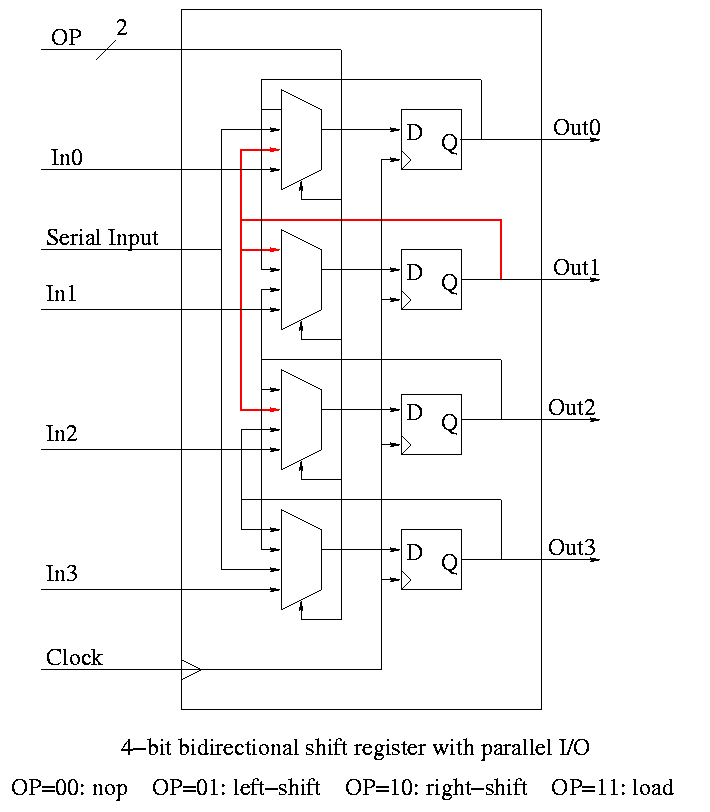
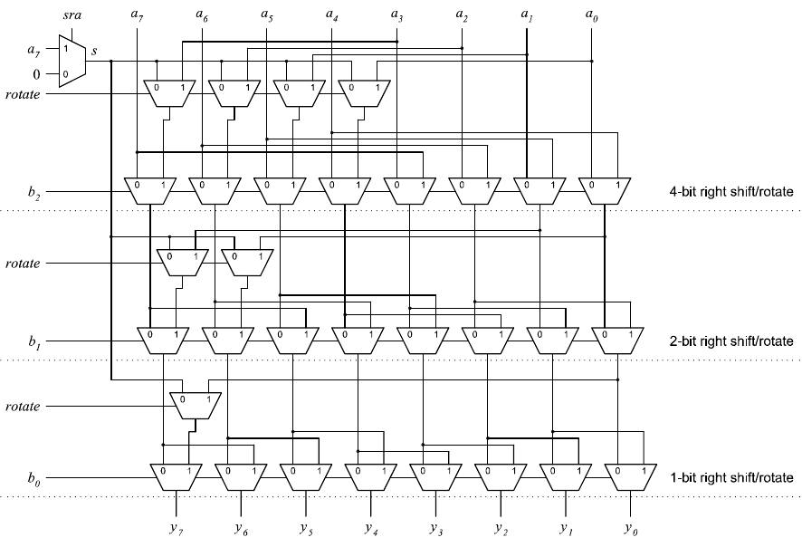
Shift register
Barrel shift/rotate
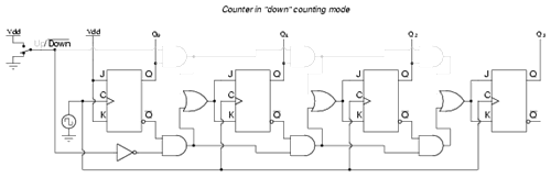
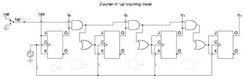
Synchronous up/down counter
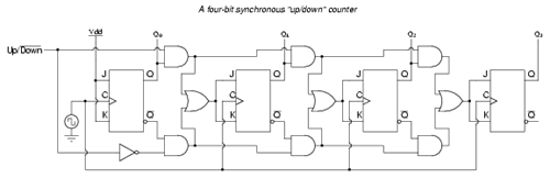
Up counting
Down counting